1. Material Fundamentals and Structural Qualities of Alumina Ceramics
1.1 Crystallographic and Compositional Basis of α-Alumina
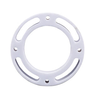
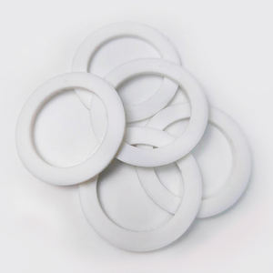
(Alumina Ceramic Substrates)
Alumina ceramic substrates, mostly made up of light weight aluminum oxide (Al two O FIVE), function as the backbone of modern-day electronic product packaging because of their outstanding equilibrium of electric insulation, thermal stability, mechanical strength, and manufacturability.
One of the most thermodynamically stable stage of alumina at high temperatures is diamond, or α-Al ₂ O FIVE, which crystallizes in a hexagonal close-packed oxygen lattice with aluminum ions occupying two-thirds of the octahedral interstitial websites.
This dense atomic plan imparts high hardness (Mohs 9), superb wear resistance, and strong chemical inertness, making α-alumina ideal for rough operating environments.
Commercial substrates typically have 90– 99.8% Al ₂ O SIX, with minor additions of silica (SiO TWO), magnesia (MgO), or rare planet oxides utilized as sintering aids to promote densification and control grain development throughout high-temperature handling.
Higher pureness qualities (e.g., 99.5% and over) exhibit remarkable electric resistivity and thermal conductivity, while reduced purity versions (90– 96%) use cost-effective solutions for much less requiring applications.
1.2 Microstructure and Defect Design for Electronic Reliability
The performance of alumina substrates in digital systems is critically based on microstructural uniformity and issue reduction.
A fine, equiaxed grain structure– normally ranging from 1 to 10 micrometers– makes sure mechanical integrity and minimizes the chance of fracture breeding under thermal or mechanical anxiety.
Porosity, particularly interconnected or surface-connected pores, should be lessened as it breaks down both mechanical stamina and dielectric performance.
Advanced handling strategies such as tape spreading, isostatic pressing, and controlled sintering in air or managed environments allow the manufacturing of substratums with near-theoretical thickness (> 99.5%) and surface roughness listed below 0.5 µm, essential for thin-film metallization and cable bonding.
Additionally, impurity partition at grain boundaries can cause leakage currents or electrochemical movement under prejudice, requiring rigorous control over resources purity and sintering problems to guarantee lasting dependability in damp or high-voltage environments.
2. Production Processes and Substratum Construction Technologies
( Alumina Ceramic Substrates)
2.1 Tape Casting and Environment-friendly Body Processing
The manufacturing of alumina ceramic substratums starts with the preparation of a very distributed slurry including submicron Al two O four powder, organic binders, plasticizers, dispersants, and solvents.
This slurry is refined using tape casting– a continuous method where the suspension is spread over a moving carrier film making use of an accuracy doctor blade to achieve uniform thickness, normally between 0.1 mm and 1.0 mm.
After solvent dissipation, the resulting “eco-friendly tape” is flexible and can be punched, drilled, or laser-cut to develop through holes for vertical affiliations.
Several layers might be laminated flooring to develop multilayer substratums for complicated circuit assimilation, although the majority of commercial applications make use of single-layer setups because of cost and thermal growth considerations.
The eco-friendly tapes are then meticulously debound to remove natural ingredients with regulated thermal decay before final sintering.
2.2 Sintering and Metallization for Circuit Combination
Sintering is carried out in air at temperatures in between 1550 ° C and 1650 ° C, where solid-state diffusion drives pore elimination and grain coarsening to achieve complete densification.
The direct contraction during sintering– generally 15– 20%– need to be specifically predicted and made up for in the design of environment-friendly tapes to make certain dimensional accuracy of the final substrate.
Following sintering, metallization is applied to form conductive traces, pads, and vias.
Two primary approaches control: thick-film printing and thin-film deposition.
In thick-film technology, pastes containing steel powders (e.g., tungsten, molybdenum, or silver-palladium alloys) are screen-printed onto the substratum and co-fired in a decreasing atmosphere to create robust, high-adhesion conductors.
For high-density or high-frequency applications, thin-film procedures such as sputtering or evaporation are utilized to deposit bond layers (e.g., titanium or chromium) adhered to by copper or gold, making it possible for sub-micron patterning using photolithography.
Vias are full of conductive pastes and terminated to establish electrical affiliations between layers in multilayer layouts.
3. Functional Properties and Efficiency Metrics in Electronic Equipment
3.1 Thermal and Electric Actions Under Functional Stress And Anxiety
Alumina substrates are prized for their favorable combination of moderate thermal conductivity (20– 35 W/m · K for 96– 99.8% Al ₂ O TWO), which enables efficient heat dissipation from power devices, and high volume resistivity (> 10 ¹⁴ Ω · cm), making certain marginal leak current.
Their dielectric continuous (εᵣ ≈ 9– 10 at 1 MHz) is stable over a wide temperature and frequency variety, making them suitable for high-frequency circuits approximately several ghzs, although lower-κ products like light weight aluminum nitride are chosen for mm-wave applications.
The coefficient of thermal development (CTE) of alumina (~ 6.8– 7.2 ppm/K) is fairly well-matched to that of silicon (~ 3 ppm/K) and specific packaging alloys, decreasing thermo-mechanical anxiety during device operation and thermal biking.
Nonetheless, the CTE mismatch with silicon continues to be a worry in flip-chip and direct die-attach configurations, usually calling for compliant interposers or underfill materials to alleviate tiredness failure.
3.2 Mechanical Robustness and Ecological Longevity
Mechanically, alumina substratums exhibit high flexural strength (300– 400 MPa) and excellent dimensional stability under load, enabling their use in ruggedized electronic devices for aerospace, auto, and commercial control systems.
They are resistant to resonance, shock, and creep at elevated temperature levels, preserving architectural stability approximately 1500 ° C in inert environments.
In humid atmospheres, high-purity alumina shows marginal wetness absorption and superb resistance to ion migration, ensuring long-term integrity in outside and high-humidity applications.
Surface firmness additionally secures versus mechanical damages throughout handling and assembly, although care should be taken to prevent edge cracking due to integral brittleness.
4. Industrial Applications and Technological Impact Across Sectors
4.1 Power Electronic Devices, RF Modules, and Automotive Systems
Alumina ceramic substrates are common in power digital components, consisting of protected gate bipolar transistors (IGBTs), MOSFETs, and rectifiers, where they provide electric isolation while facilitating warmth transfer to warm sinks.
In superhigh frequency (RF) and microwave circuits, they act as provider systems for crossbreed integrated circuits (HICs), surface acoustic wave (SAW) filters, and antenna feed networks due to their stable dielectric properties and low loss tangent.
In the automotive industry, alumina substratums are utilized in engine control units (ECUs), sensor packages, and electrical car (EV) power converters, where they endure high temperatures, thermal biking, and exposure to corrosive fluids.
Their dependability under severe conditions makes them important for safety-critical systems such as anti-lock braking (ABDOMINAL) and progressed vehicle driver support systems (ADAS).
4.2 Clinical Tools, Aerospace, and Arising Micro-Electro-Mechanical Systems
Beyond customer and industrial electronics, alumina substrates are used in implantable medical gadgets such as pacemakers and neurostimulators, where hermetic sealing and biocompatibility are paramount.
In aerospace and defense, they are used in avionics, radar systems, and satellite communication modules as a result of their radiation resistance and stability in vacuum cleaner environments.
Furthermore, alumina is increasingly utilized as an architectural and shielding system in micro-electro-mechanical systems (MEMS), including pressure sensing units, accelerometers, and microfluidic tools, where its chemical inertness and compatibility with thin-film handling are helpful.
As digital systems remain to require higher power thickness, miniaturization, and reliability under severe problems, alumina ceramic substrates continue to be a keystone product, linking the gap between efficiency, price, and manufacturability in sophisticated digital product packaging.
5. Distributor
Alumina Technology Co., Ltd focus on the research and development, production and sales of aluminum oxide powder, aluminum oxide products, aluminum oxide crucible, etc., serving the electronics, ceramics, chemical and other industries. Since its establishment in 2005, the company has been committed to providing customers with the best products and services. If you are looking for high quality nano alumina, please feel free to contact us. (nanotrun@yahoo.com)
Tags: Alumina Ceramic Substrates, Alumina Ceramics, alumina
All articles and pictures are from the Internet. If there are any copyright issues, please contact us in time to delete.
Inquiry us